Most conducted EMI problems are due to common mode noise. Furthermore, most common-mode noise issues are caused by parasitic capacitances in the power supply.
For Part I of this discussion, let’s focus on what happens when the parasitic capacitance couples directly to the input wires to the power supply.
1. It only takes a few fF of stray capacitance to fail an EMI scan. Switching powers supplies, by their nature, have nodes with high dV/dt. Mixing parasitic capacitance with high dV/dt creates EMI problems. When the other end of the parasitic capacitance is tied to the input of your supply, a small amount of current is pumped directly onto the power lines.
2. Visualize the parasitic capacitances in your power supply. We all remember from physics class that capacitance between two conductors is proportional to the surface area of the conductors and inversely proportional to the distance between them. Look at each node in your circuit and pay close attention to the nodes with high dV/dt. Think about how much surface area is on that node in your layout and how far it is from the input lines to your board. The drains of switching MOSFETs and snubber circuits are common offenders.
3. Decreasing surface area can be tricky. Try to use surface mount packages as much as possible. A FET in a TO-220 package standing vertically has a huge amount of surface area from the drain tab, which unfortunately, usually happens to be the node with the highest dV/dt. Try using surface mount DPAK or D2PAK FETs instead. By running a primary ground plane on the bottom PCB layer under the tab of the DPAK, the bottom side of the FET is well shielded and the parasitic capacitance is greatly reduced.
Sometimes surface area is needed for heat sinking purposes. If you must use a TO-220 style FET with a heat sink, try tying the heat sink to primary ground (not earth ground). This will help shield the FET and cut down on the stray capacitance
4. Put some distance between your switching nodes and input connections. See Figure 1 for an example of a design where I neglected to follow this simple rule.
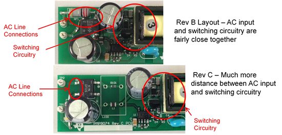
Figure 1. Routing the input connections too close to nodes with high dV/dt can increase conducted EMI.
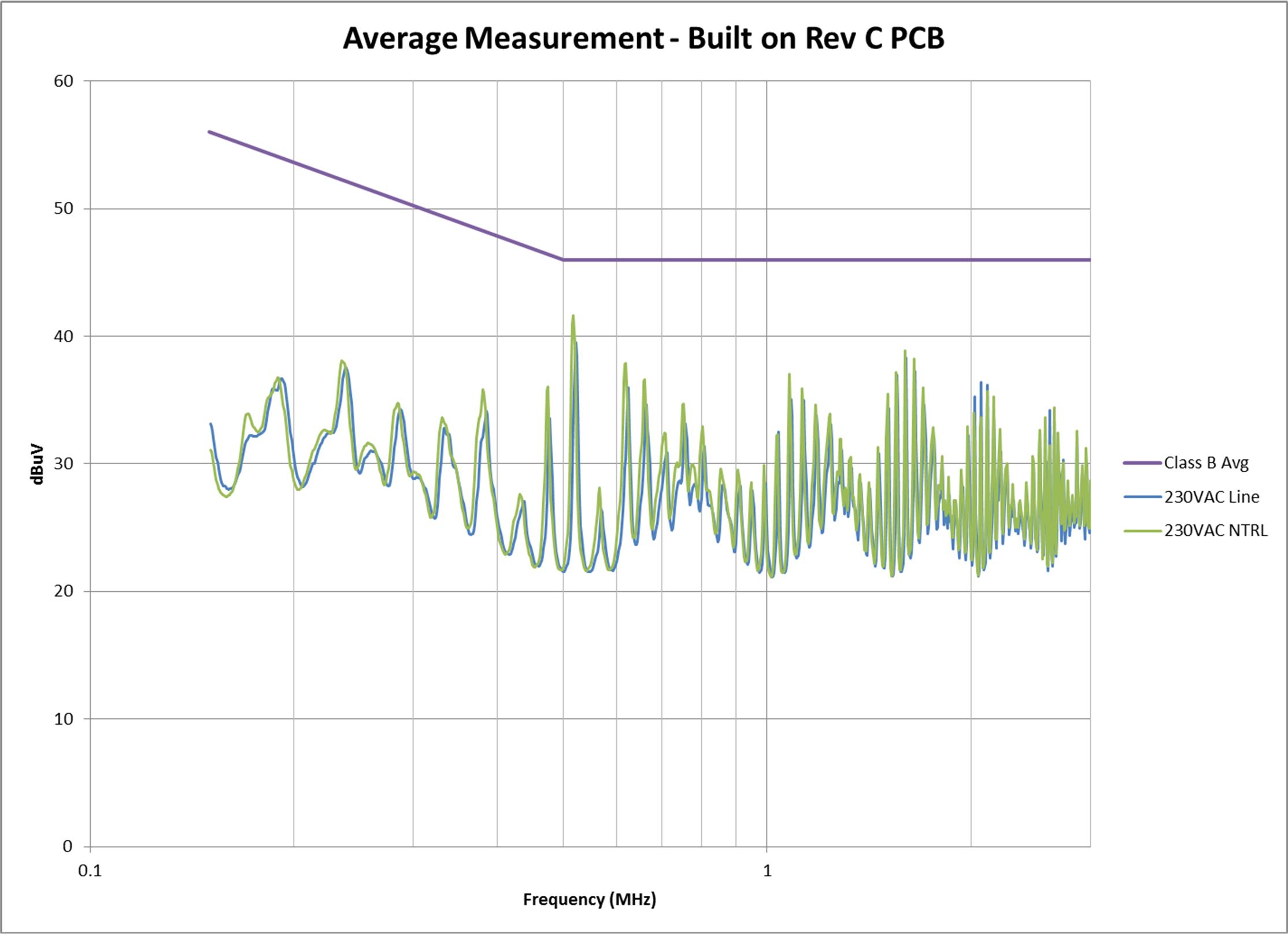
By simply relaying out the board (no circuit changes), I reduced the noise by about 6dB. See Figures 2 and 3 for the measurement results. In some cases, routing the input wires near high dV/dt can even defeat your common mode choke (CMC).
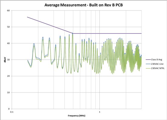
Figure 2. EMI scan from board layout where the AC input and switching circuitry are close together.
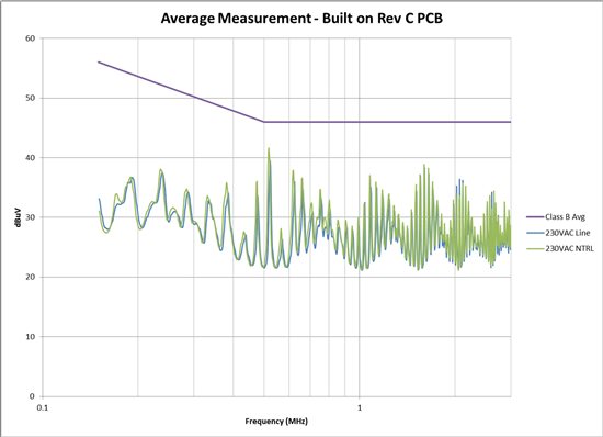
Figure 3. EMI scan from board layout where more distance was provided between the AC input and switching circuitry.
Have you been frustrated because after massively beefing up your input filter, you see little or no improvement in the EMI? This is likely because there is some stray capacitance from a node with high dV/dt coupling straight to your input lines, effectively bypassing your CMC. To test this theory, temporarily short out the windings of the CMC on your PCB, and place a second CMC in series with the input power wires feeding your board. If you see a big improvement, you need to re-layout your board and pay close attention to placement and routing of your input connections.
In part II of this topic, I’ll talk about parasitic capacitance inside the power transformer. Email subscribe (top right corner of this page) to the blog so you don’t miss it.